
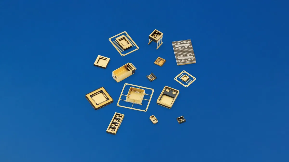
Ceramic packaging is the “housing” for sealing and protecting semiconductor chips, MEMS, or other electronic components. This effectively protects Integrated circuit packaging (ICs), senso…

Ceramic packaging is the “housing” for sealing and protecting semiconductor chips, MEMS, or other electronic components. This effectively protects Integrated circuit packaging (ICs), senso…
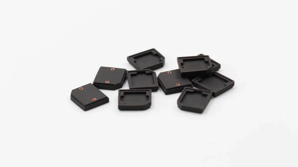
As optical communication, LiDAR, and high-precision optoelectronic detection systems evolve toward higher power and greater integration density, they place higher demands on the performance of optoele…
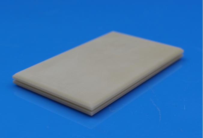
Ceramic substrates and packages are used for semiconductor packages and electronic modules, of which the speedy operation and high integration are advancing, and sensor modules, of which the high prec…
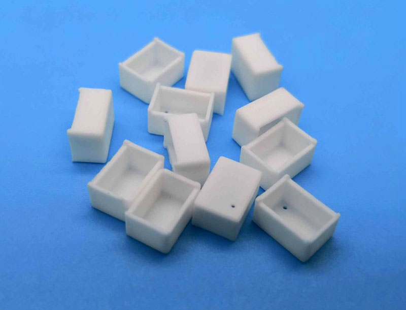
Ceramic is commonly used in packages due to its superior mechanical properties, suitable for small, high density, and surface mountable applications- including accelerometers and angular rate, pressur…
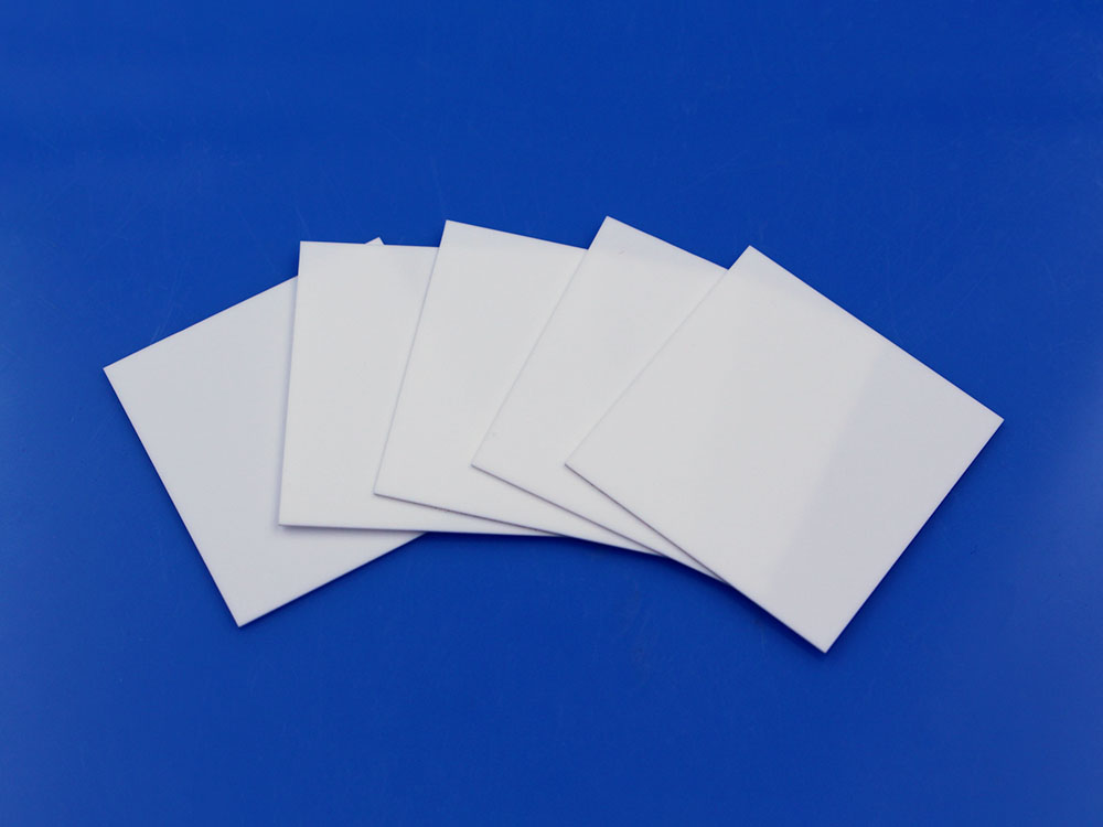
LED packaging materials are diverse, each has its own dominant field, and ceramic packaging has a dominant position in the field of the high power LED.The application of the LED ceramic Packages are a…