

Semiconductor
Ceramic components for semiconductor tools where purity, vacuum compatibility, plasma exposure and thermal stability must be reviewed together.
Engineering requirements behind Semiconductor ceramic components
Semiconductor equipment exposes components to heat, plasma, vacuum, corrosive gases, precision handling and particle-sensitive process conditions. Ceramic parts must remain stable without adding contamination or unpredictable dimensional change.
- High purity
- Vacuum compatibility
- Plasma resistance
- Thermal process stability
Where Ceramic Components Are Used in Semiconductor Equipment
Use this section to match your equipment type with typical ceramic parts and the key requirements we should review before quoting.
Wafer handling
Etch and deposition
Vacuum and thermal process
Engineering Review Notes for Semiconductor Ceramic Parts
Semiconductor ceramic components must be reviewed around process exposure, cleanliness and tool fit. A material that works in a general furnace or electrical assembly may not be suitable for a plasma, vacuum or wafer-contact environment.
Information to share before material review
- Process zone or tool location, including whether the part faces plasma, vacuum, gas flow, wafer contact or heating.
- Operating temperature, ramp rate, gas chemistry, pressure and cleaning or maintenance method.
- Drawing, critical surfaces, particle-control expectations, edge condition and surface finish target.
- Electrical insulation, thermal conductivity, thermal uniformity or dielectric performance requirements.
- Prototype, replacement or repeat-production context, including quantity and inspection needs.
How we use this information
- Check whether alumina, aluminum nitride, boron nitride, silicon carbide or another ceramic is appropriate for the process zone.
- Review whether the geometry can be fired, machined and cleaned to the required tolerance and surface condition.
- Identify features that may create particle, stress, chipping or assembly risk.
- Confirm whether the project is a custom part, replacement component or material comparison sample.
What Innovacera can support
Innovacera can support drawing review, material selection, precision ceramic machining and repeatable manufacturing for semiconductor ceramic components.
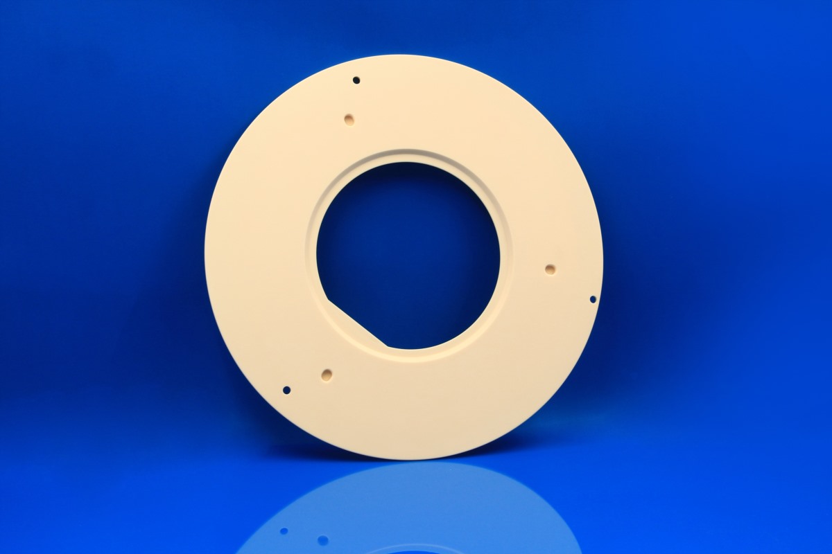
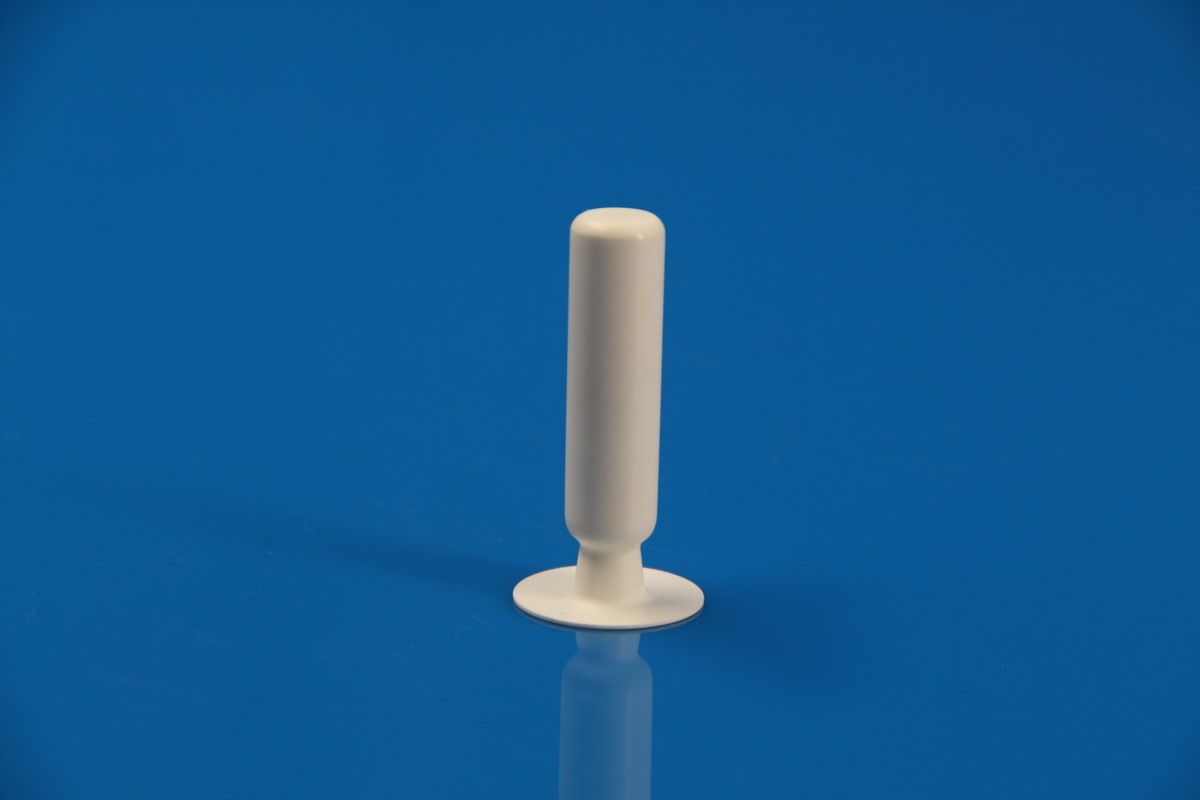
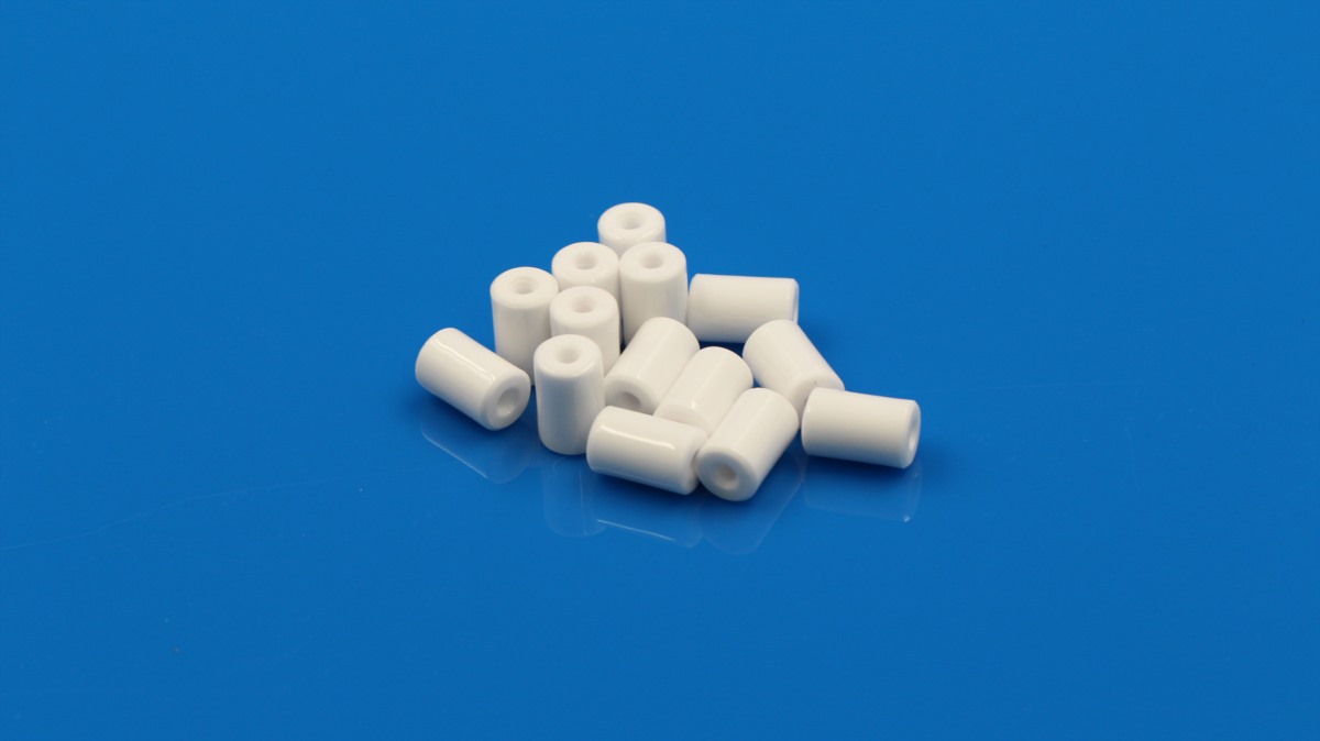
Related ceramic products.
4 related products are tagged to this application field in the current catalog. Use them as starting points for standard review or custom manufacturing discussion.

Start with the conditions. We will help review the ceramic path.
Share your operating conditions, performance requirements, and design challenges. We' Il help identify the optimal ceramic solution.