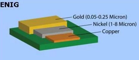
ENIG (Electroless Nickel Immersion Gold) is a surface plating that is applied over the copper pads on a Printed Circuit Board to protect them from corrosion and other abnormalities. Initially, the copper pad is covered by a Nickel (Ni) layer followed by a thin immersion Gold (Au) layer. ENIG provides good oxidation resistance, and excellent surface planarity and allows for easy soldering which results in excellent electrical performance of the PCB board.
What is ENIG Plating PCB Substrates
ENIG is one of the most used PCB surface finishes. And it is more complex and expensive when compared to other PCB plating processes like HASL.
ENIG is a two-layer metallic coating – Nickle is the barrier to the copper pad and is also the material to which components are soldered. Gold on the other hand protects the Nickle during storage and also provides low contact resistance. Typical Nickle thickness varies from 4 – 7 µm and Gold thickness varies from 0.05 – 0 23 µm. ENIG requires a processing temperature of around 80 °C.

What is ENIG Plating PCB Substrates
Advantages of ENIG Surface Finishes:
- It provides impressive wettability, surface planarity, coplanarity, and long shelf life (up to 12 months) to the PCB board since immersion gold has strong chemical properties.
- In ENIG, the nickel layer acts as a barrier and stops the interfusion between gold and copper. It also produces an intermetallic compound (IMC) Ni3Sn4 to provide good solderability after reacting with Tin.
- It has low contact resistance, high strength, reduces oxidation, and provides anti-friction. Overall, it enhances circuit conductivity requirements.
- It provides good plating over the copper pads and via holes.
- Its excellent surface planarity allows the components to be soldered flat onto the pad, making it ideal for BGA pads and other fine-pitch components.
Limitations of ENIG Surface Finishes:
- ENIG is an expensive surface finish technology
- It has undesirable magnetic properties
- Not good for rework and makes PCB repair very difficult
The metallized ceramic is used in critical assemblies brazed. Innovacera as a metallized ceramics supplier, provides you with custom services for metallized ceramic parts.
Welcome to contact us if you are interested.

PCB Substrate

