Ceramic Micropore Chuck Table adopts microporous ceramic material by special technology, which has uniform pore size distribution, and internal interconnection. After grinding, the surface is smooth and delicate and has good flatness.
It is widely used in semiconductors, electronic Devices, film products, and other industries that require vacuum chuck equipment.
The following are detailed application cases
1. Semiconductor and Microelectronics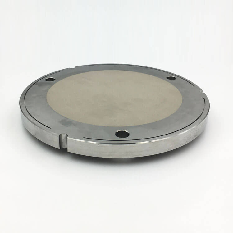
. Wafer cut.
. Wafer grinding.
. Wafer cleaning.
. Wafer AOI detection.
2. Display panel and mobile electronics
.LCD release film, AOI detection.
.OLED laser cutting, AOI detection.
.Touch Panel OCA fit.
3. Photovoltaic and new energy
.Photovoltaic film transfer and lamination.
.Fixed by laser welding.
.Single/polysilicon handling.
4. Flexible circuit
.PI film transfer and lamination.
.PI film AOI detection.
5. Precision Manufacturing
.Visual detection fixed.
.Laser processing fixed.
.Metal foil handling and fixing.
.Transport and fix in the vacuum chamber.
.Handling and fixing of fragile materials.
.Porous and breathable material handling and fixing.
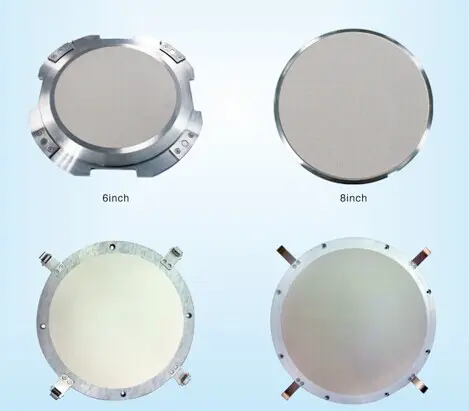
Ceramic Micropore Chuck

