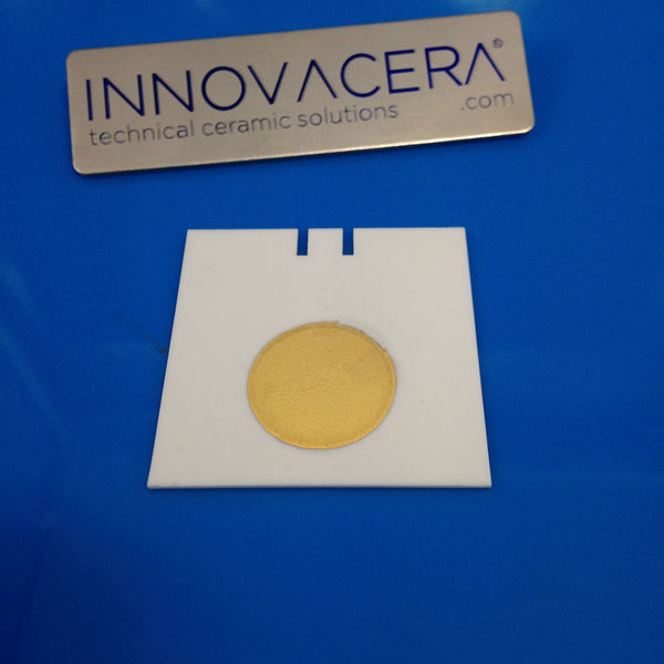
DBC Ceramic Substrate Specifications:
- Material: 96% Alumina + Cu/Ag Coating.
- Max Size: 138*188mm
- Thickness: 0.25-1.0mm (0.25, 0.38, 0.5, 0.63, 0.76, 1.0mm).
General Size:
- 2″*2″(50.8*50.8mm)
- 3″*3″(76.2*76.2mm)
- 4″*4″(101.6*101.6mm)
- 4.5″*4.5″(114.3*114.3mm)
- 5″*5″(127*127mm)
- 5″*5.5″(127*139.7mm)
- 5.4″*7.4″ (138*188mm)
Advantages:
- Low thermal resistance.
- Excellent insulation properties
- Reduce solder layers, lower thermal resistance, reduce cavities, increase the rate of finished products.
- Avoid withstand the stress caused by the impact of temperature changes, thus greatly extend the life of semiconductor products.
- The new packaging and assembly methods can be realized with DBC substrates, it makes the products a higher degrees of integration and volume reduction.
- The thermal expansion coefficient close to silicon in the semiconductor chip, it can directly solder on the DBC substrate, saving the interface layer Mo plate and then decrease the cost.
Application:
- Solar-panel array
- Solid-state relays
- Electronic heating devices
- Smartpower building blocks
- Power Semiconductor Modules
- Laser Industrial electronics
- Semiconductor refrig-erators
- Power control circuits, power hybrids.
- High frequency switch mode power supplies
- Telecommunication private branch exchange and receiving system.
- Building blocks for automobile electronics, the aerospace technology.

